Printed circuit boards (PCBs) are used in a wide variety of electronic equipment. PCBs are everywhere. They’re in your laptop, your phone, your microwave, even your light bulb.
So what is a PCB?
It is essentially a board that connects electronic components and is the basic building block of any electronic design.
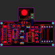
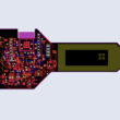
Checkout some examples of PCB projects:
Opensource electronics design database | Inventhub
In designing a PCB of a product, there are a lot of stages before the final product is ready for manufacturing. The process of design starts with requirements research and ends with a product that’s ready for production. There are different types of hardware products like complex machines, industrial equipments and consumer gadgets that go through their own processes depending on what they are supposed to do but the general steps involved are:
Planning Research and building POC (proof of concept)
This is where information is compiled that goes into designing the PCB, which creates a set of requirements to build out a proof of concept. A schematic capture is the first step as the logic representation of the PCB. It consists of the industry standard components represented as symbols. Before this leads to a PCB layout, its a good idea to review schematic design rule checks (DRCs) and making sure that all the library versions of components are updated.
Design and its verification
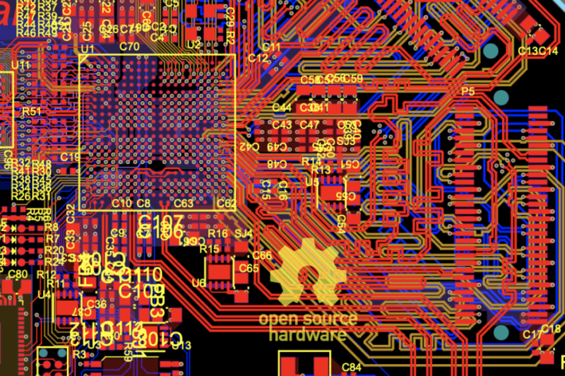
PCB Layout is the physical design of the schematic symbols and the nets. For this the board outline needs to be set with how many layers the board will have in it and in what order they are to be stacked up. The symbols in the schematic capture would now be associated with the PCB footprints. With an ECAD tool the design is created with fixed parts like connectors and switches, critical parts like power supplies and core chips, supporting parts like resistors, inductor and capacitors that complements the associated critical parts and the remaining parts to complete the whole PCB. Component placement in this phase is crucial to make sure the board is ready for manufacturing. When doing trace routing, trace sizes and signal integrity should be viewed carefully. For this various PCB trace design rules can be setup that specify width and spacing, area rules, layer routing directions and signal path rules for high speed design. It is a good idea to understand design for manufacturing (DFM) which helps in production costs.
Bill of materials
The symbols in schematic capture have a physical place on the PCB and these components are reported in the bill of material. The bill of materials has the full information of the components used on the PCB like Manufacturer Part Number (MPN), descriptions, quantities, and reference designators. BOMs can be created manually but mostly they are computer generated and is an evolving document as the PCB design evolves. Maintaining this involves various stake holders like procurement, suppliers, and manufactures.
Manufacturing and Production Validation
Before going into manufacturing, test fixtures need to be created through test documentation that is compiled during designing. Make sure silkscreen markings are laid out in the ECAD tool that you use for PCB design. Its a good idea to work with your manufacturer for best practices for creating PCB silkscreen before going to production. This helps maintenance, setups and field repairs that require simple information printed on the PCB. Make sure fabrication and assembly drawings notes are spotted correctly by the manufacturer. This includes non-standard board feature, mounting instructions, drill information, solder mask colour and specific layer dimensions. All of the information linked to the PCB Design must go through a checklist with your manufacturer that would not cause any issues with manufacturing. This might include board image files, IPC netlist, gerber files, list of critical components that have special fabrication, assembly, test requirement, or are unique and require special order.
As the design processes evolves and to get products to the market as fast as possible, you have to experiment with new designs and their different attributes.
Here are two things that should be at the core of the design process:
Collaboration
Building the PCB design of a product goes through various iterations and that is where early communication is needed. Each stage of the process involves a stakeholder that helps in moving the product close to production. This helps in conducting design reviews and share feedback between outside collaborators like customers, manufacturers/suppliers and the people you work with.
Data Management
When going through all the iterations of a design, how you manage your data is crucial. You can use a tool or create a centralized, secure, cohesive and intelligent electronics project database. Having one database to do multiple reads and writes helps everyone to have the same version of the design documents. This organizes design and component data, helps search information, create project history and track revisions. The result of this is to have up-to-date design assets from anywhere, while enabling everyone to reuse design information in future projects.
Here are some advantages when collaboration and data management are at the core the design process:
- Bring flexibility to unstructured change processes.
- Systematically introduce major and minor changes into projects.
- Avoid collaboration bottlenecks and missed deadlines, collaboratively design electronics product leading faster to market.
- Avoid costs and save time spent on failed prototypes.
- Deliver high quality products with collaborative design reviews and transparent updates.
- Enable easier access to design data, build cohesive design history and increase reusability with version controlled secure storage.
PCB design software that are out there:
- Autodesk Eagle
- Altium Designer
- KiCAD
- Cadence
Checkout how https://inventhub.io tackles PCB design collaboration and data management.
Refs: