What is a high-frequency PCB? The short answer, while not 100% accurate, is a PCB tuned for high frequency applications. But what does that really mean? And why do we care? It means that certain design techniques and materials were used in the manufacture of the board to deal with the challenges presented by running at high frequencies. Typically this means matching networks, decoupling capacitors, and low ESR ceramic capacitors. The material choices also often include FR4 (Teflon and fiberglass), and sometimes metal core and copper pour ground planes.

What are the characteristics of a High Speed Printed Circuit Board Design?
High speed PCBs have a number of key design characteristics:
- It uses high speed interfaces for fast data transfer, such as HDMI, Ethernet, SATA, PCI Express, USB, Thunderbolt, or other interfaces.
- Circuit and its sub-circuits connected together through high speed interfaces (LVDS, DSI, CSI, SDIO, DDR3, etc.)
- A rise time of at least ⅓ signal propagation time is the minimum required for the track integrity.
- The frequency of digital signals is usually at least 50MH or higher.
- The tiny size of the printed circuit board makes it difficult to place the components, especially if you need to conform to a high-speed interface standard.
When working at high frequencies, high speed PCB design is applied to devices with the use of high speed interfaces. With that much data and speed of transfer, and given how dependent board design and manufacturing has become on computer-aided design (CAD) there are lot of things to deal with in getting the right results.
Preparing Your Design for High-Frequency PCB Layout:
The best way to approach high speed design is to start small. Fast components often need fast tools and test equipment. Components commonly used in high speed digital circuits include microcontrollers, FPGAs, RF and MCU transceivers, and many other components. The cool thing about using these components is that manufacturers typically release development boards for them. These development boards usually cost only a few hundred dollars. Developers use development boards to quickly prototype designs and test new chips before moving to a full board layout.
If you want to experiment with any of the high speed devices, it becomes impractical to layout your board in an arbitrary way. You need to follow high speed design guidelines.
If you can lay down a bunch of electronic components on top of a development board and they work properly, then you should be able to lay your new board out however you want as long as it follows the same stackup design as your development board. In many cases, this won’t be possible, and you’ll need to integrate everything into a single PCB.
In general, high speed devices require careful design of components to meet electrical standards. High speed components often work best on a board where the designers have had the freedom to select all the component package, size, and spacing to meet a particular electrical specification. If a development board for a device you are interested in does not exist, you might find it helpful to design your own development board which you can put together with your very own hands on a breadboard. However, breadboards are not a place to implement high speed device circuits.
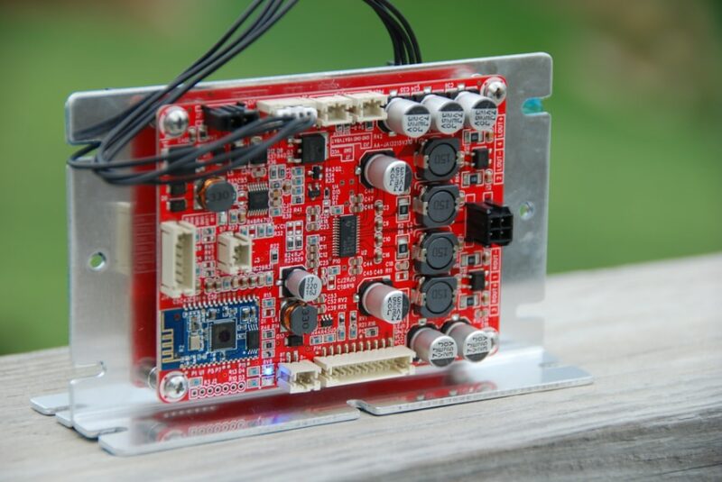
A High Speed PCB:
High speed designs are becoming increasingly common. Back in the day, the main problem designers faced was how to get all of their components on a single board and how to get all of them connected without any bits and pieces getting in the way. And it’s no surprise that an increase in speeds also meant an increase in complexity. The EMI standards we need to adhere to ensure we don’t produce excessive noise while our conductors and insulators need to be thick enough to reduce signal reflections.
There is no clear delineation between a high speed board and a low speed board, and any new design should be designed with high speed board design guidelines in mind.
If the rise time of high speed pcbs is fast enough then the digital signal bandwidth can be in the high MHz or GHz frequencies. And if the board is not designed using high speed pcb design rules then certain signal distortions or problems can occur.
Some high speed board design guidelines included below will help you combat signal integrity and power integrity problems.
Component Placement
High frequency PCB design is the act of optimizing PCB traces to transmit RF signals with minimal reflection and to maximize signal integrity. This goes way beyond the basics of just keeping track of impedance limitations. There are many factors that must be considered when deciding where to place components on a PCB, especially prior to laying out the first trace. The goal here is to design high quality PCBs which can minimize insertion loss, maximize isolation between adjacent channels, and reduce crosstalk from adjacent channels.
When designing a board layout, pay attention to spacing between components. PCBs can be ruined because of component placements, which leads to poor quality PCB design. This ultimately leads to malfunctions.
Impedance Control in PCB Design
Signals that take longer than 5 ns to reach their final value from a starting point will travel slower than the speed that the signal is designed for. This will create an impedance mismatch that can cause reflections that mess up the integrity of the digital signal. Keeping a low rise time in your design will allow your signal to reach its highest possible velocity, thereby minimizing impedance mismatches and resulting reflections.
Rise time in high speed pcb boards can be shorter than its critical rise time and that depends on the length on an interconnect which is followed by a dependence on maintained or allowed impedance mismatch at the ends of an interconnect.
When you design with impedance controlled routing, your board is designed for minimum reflections and incorrect terminations. It enhances signal integrity and reduces electromagnetic interference (EMI). If your traces are too long, impedance control needs to be used, where you route the trace with specified impedance. This is done by adjusting the geometry of your traces such that they take a target value (impedance). The routing should have a clear signal return path available on an adjacent reference plane layer, and should not route high-frequency lines across any splits in the reference plane. Power plan can be a bit smaller to avoid any coupling on the edges of the board between power and ground planes. This is when power and ground planes are on adjacent layers of the board.
Your Board Stackup for Manufacturing
The layers of your circuit board stackup affect the properties of the signals it transmits. For example, high-speed digital signals require an unbroken ground plane beneath them so their loop inductance is low, which in turn improves signal integrity. Your stackup will have a large impact on signal integrity and power integrity. A nearby reference plane (power or ground) should be on an adjacent layer.
Try routing all high speed signals of the pcb board on the inner layers between planes, which shields against external emitted radiation.
Try using multiple ground planes in layer stack up. This assists in lowering your reference impedance and reduces common-mode radiation that could affect your circuit.
Power Integrity in High Speed PCBs
A well designed power integrity scheme can be the key factor in getting optimum performance, meeting EMC requirements and avoiding costly failures. With increased demands for increased speeds, increased functionality, lower power consumption, higher levels of integration, less design time to market using pre-qualified components and cost pressure, understanding the factors involved will have a huge advantage.
One common problem in a poorly designed digital board is a power drop when processor components are running at high clock rate. The sudden high-frequency current drawn from a regulator can create a strong power transient because of the switching of multiple gates. This problem manifests as components either failing to operate at normal speed or being entirely inaccessible.
High speed PCB design is difficult because the power delivery network (PDN) has a non-linear impedance response. The main challenge is that the network can’t keep up with the high frequency switching of modern digital circuits. This is both a problem in digital and analog, and it’s much more difficult to solve in the digital domain. Analog signals are less wide as compared to digital signals bandwidths and in the PDN impedance spectrum the signals can span on multiple resonances.
At first glance, using decoupling capacitors might seem a good way to reduce power integrity problems in digital devices. However, a power network should be analyzed for PDN impedance, and high interplane capacitance can lower it (in addition to the use of decoupling capacitors). Low PDN impedance will keep transient ripple on the PDN low. And phase noise (i.e., jitter) on the signal’s output from a component is reduced.
When starting out with your high speed design process, you will have to be either skilled or work with an expert as there are many setbacks and iterations. Before designing and having a plan for the process make sure you are able to ask yourself some questions to get you started:
- System organization – Do I have a visual diagram that will help me to visualize how all of my sub-circuits interconnect and a well-established return current?
- Signal speed and velocity – Do I know the highest frequency and fastest rise time of each signal?
- Power supply – Have I documented every one of my voltage and power requirements for all of my ICs, and will I need to split any power planes?
- Requirements for Sensitive signals – Do I have a plan to meet their needs for differential signals, controlled impedance, and trace length or propagation?
These won’t be your only questions and this where the need to work with your manufacturers, suppliers and other stakeholders arises. Gathering and building up on minimum requirements with regards to tolerance, routing, and tracing etc along with their variations would be up for discussions. High Speed Digital Design would also help understanding the process.
Design Challenges in High Frequency PCBs
As discussed above, all of the challenges involved with high frequency PCBs are related to maintaining signal integrity and to some extent power integrity. Another problem that occurs with digital circuits is timing. Matching and adding the received signals at the time of decision to improve the quality of the signal. With that a hybrid circuit design can also be a problem for interfaces between RF, IF, and LF circuits. Electrostatic Discharge (ESD) can also still occur, so ESD characteristics should also be considered.
ECAD Software Helpful Features
A commonly overlooked aspect of high speed PCB design is the importance of using high speed CAD software to capture the schematics and layout of your electronics. Among various ECAD softwares like Altium Designer, EAGLE, Cadence Allegro, KiCad, and others, Altium designer facilitates a high speed layout design to a large extent. Altium has a Propagation Delay function for high speed PCB design, which is useful for designers interested in the length of signal traces and the signal propagation delay at the same time.
The Propagation Delay function helps when specific signal delay is needed on a specific track. A rule in Design Rule Check (DRC) can be set for checking if preset conditions are met on selected tracks, for example, minimizing the delay difference between differential pairs.
Interactive Sliding in altium also tackles issues in high speed layout. It helps in the design of various non-standard printed circuit boards, like star or ring shaped PCBs.
Quick tips for high-speed PCB designers
- Determine what net has the highest frequency and determine how fast the signal rises and falls in the circuit.
- Ensure that the electrical specifications at the inputs and outputs of the sinks and sources are within an acceptable range.
- Ask yourself a few questions about impedance, termination, and propagation delay on a trace. Is impedance really as straightforward as it sounds? And why is controlled impedance so important?
- Choose between microstrip and stripline routing techniques for board assembly.. Simulate the circuit for more EMC-compliance that can give better signal integrity results.
- Clock and differential routing techniques help in quality signal transmission.
- Different supply voltages in the circuit can have their power plane, or can be split.
- Figure out how to show all of the parts like the transmitter path, receiver path, analog signals, digital signals, etc. and label each part with its function.
- Check interconnections between independent functional groups to see return current and crosstalk to other traces.
- Ensure width, minimum distance between the layers, space of parts and clearance
- Check minimum drill and via requirements for use of blind and buried vias.
High speed PCB Materials
FR-4, a common laminate material is economical with circuit board frequencies that are in between a range of 2.5 to 3 GHz. With high speed, if FR-4 type material is not used then it can be very expensive although materials like Rogers RO4350 have better properties than FR-4.
PCB signal velocity depends on its dielectric constant. For example, at frequencies greater than 5 GHz, FR-4 dielectric constant drops to 4 from 4.7 where as its constant for Rogers RO4350 till 15 GHz which is 3.5. So different velocities can exist and reach loads at different times causing signal distortion with different frequency components when the dielectric constant of PCBkeep changing with the frequency.
New Solutions with High Speed Design
If you’re involved in a high speed PCB design project as your first endeavor, you’ll be learning a lot about it with new issues as you go alongThe simple idea of just fitting the pieces together no longer suffices. You have to be concerned about the signals where they originated, and how they affected or will affect parts of your circuit. The gist of this is that there’s problems with electromagnetic interference (EMI). When you learn more about high-speed design, you’ll learn how to address EMI/EMC or electromagnetic compatibility issues with specific techniques and strategies. So consider the above guidelines just enough to get you started on your first project.
Building anything new is exciting, but when it comes to PCB design, there are many different steps that are inevitable. Perhaps you have a small team or a big one. Either way, this isn’t something that should be rushed. High speed PCB design not only requires great vision but results in a flawless execution. Circling back to the design concept, there are multiple factors in this sector that need your attention. And when you‘re running short on time, these details can wreak havoc on your project.
Have a look at how Inventhub can help you in managing all your electronics design resources and collaborate with all participants and stakeholders involved.


