
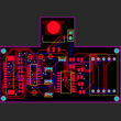
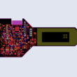
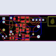
A multilayer printed circuit board, or PCB, is a circuit board with a layer of insulating material between two or more layers of conducting material. Multilayer PCBs support a higher density of electronic components and provide a greater degree of electrical isolation than single-layer boards.

Importance of PCB Manufacturing process and Multilayer PCBs:
The PCB manufacturing process is the most critical task in determining the success or failure of any product or technology, given that it involves people, time, money and other aspects. It is also the most complex stage in the electronics development cycle. Hence, a considerable amount of time needs to be devoted towards planning, organizing and managing this process.
The PCB manufacturing process can be broken down into three major phases: designing, manufacturing and quality control. There are a lot of people involved along the way and it is not without its problems.
The Multilayer PCB manufacturing process is commonly used to reduce the costs and hence improve ‘time to market’. Its applications can be found in verticals like consumer, industrial, and medical electronics.
As we have seen, semiconductor components have considerably revolutionized the electronics industry in recent time due to their ability to withstand higher temperatures when subjected to the manufacturing process of PCBs. Electronics devices get more compact with every passing year. The size of PCBs along with the processor size plays a crucial role in making them more slim and efficient.
There are different forms of PCBs:
- Single and Double layer
- Multilayer
- Rigid
- Flexible
- Aluminum back
- Rigid-flex pcb
Multilayer PCBs give you more wiring area than most other types of PCBs. By combining two or more single or double sided PCBs into one, you can get a larger number of connections without losing any space within the board.
Components Used in the Construction of Multiple PCBs:
- Led: The Led lets current flow in a direction
- Capacitor: It is made up of an electrical charge
- Transistor: Utilized in amplifying charge
- Resistors: It helps in controlling the electric current when it passes through
- Diode: Diodes allow the passing of current through one direction only
- Battery: its gives the circuit its voltage
- Hydraulic press: This ensures that metallic objects are transformed into metal sheets. This helps during thinning when making glass powder, as well as tablets making.
- Prepreg: This is an important material utilized in multilayer boards. They help in holding the cores together. Prepregs are made up of fiberglass, which is impregnated with an epoxy-based material known as resin. Its layers are compact at a specific temperature. This helps in creating a specific board thickness.
Designing a Multilayer PCB:
Designing a multi-layer pcb like either a 4 layer pcb or a 6 layer pcb requires designers to construct a circuit layout of the product first. The schematic diagram gives an understanding of the components and their connections.
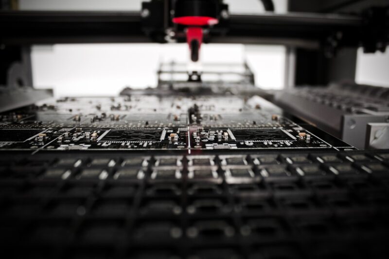
Its manufacturing process involves stacking consecutively formed PCBs called Laminate (which is produced as a single layer PCB) which provides shielding and isolation between layers.
Inner copper layers are laminated using a process called prepreg. The prepreg is mixed with resin and applied to a fabric in precise thickness. The fabric is then placed into a machine that applies heat and pressure to form the laminate. This lamination process is critical to ensure that the layers are correct. A small error here will cause a large amount of noise or even a short circuit. The “Masking” layer after the lamination process prevents pcb boards from ESD and oxidation.
One thing to remember is that the cost of the PCB manufacturing increases with the number of PCB layers.
For pcb manufacturers to get the circuit design to a physical form a gerber file is needed which is generated from any of the ecad software a designer uses.
The process for manufacturing multilayer PCB involves most of the following steps:
- Developing the Desired Design, to ensure that all aspects of your design are error-free, it’s important that you plan the layout of your PCB, then encode everything according to the requirements. Finally, once the layout is complete, your PCB is ready to be fabricated.
- Printing of the PCB Design, the earliest part of the printing process comes after designing is finished. as that will let you concentrate on aligning the films as you continue.
- Black Oxidation, the boards with inner layer wiring are blackened or browned before they can be laminated. It is to oxidize the copper surface of the inner layer board. Generally generated Cu20 is red.
- Pressing, lamination should be in symmetry. Because the board will be affected by pressure and temperature during the lamination process, there will be stress in the board after lamination. The thickness of the resin part is determined by the copper content. If the copper distribution is uneven, it will cause the resin flow rate at each point to be different, so that the thickness of the place where the copper is less will be slightly thinner.
- Drilling and PCB Plating, this process helps in fusing the different PCB layers making use of a chemical. Before you drill, the drill spot is located with an x-ray machine. This helps in securing the PCB stack. PCB plating is done to make sure that the soldering of the components can be achieved and completing silk-screening.
- Electrical and Testing Reliability, The electronic test is the electrical performance test of the PCB, which is usually also called the “on” and “off” test of the PCB. Among the electrical test methods used by PCB manufacturers, needle bed test and flying probe test are the most commonly used.
- Profiling and cutting, different PCBs are cut from the initial panels, and they are delivered after the inspections.
Multilayer PCB Quality Standards:
ISO 9001 is a quality management standard to promote manufacturers to meet the needs and exceed expectations of customers by effectively improving the quality of products in an efficient manner.
IATF16949 is a set of quality management standards which requires quality, security, reliability and performance of automotive products.
The UL listing service requires tests and specific requirements to be met from manufactures.
RoHS a series of restrictions for the use of 6 hazardous substances and requires manufacturers to specify maximum concentration for each type of restricted substance and practical concentration should never be higher than that.
Advantages and disadvantages of PCB Multilayer pcb manufacturing process
Disadvantages:
- Higher power – There are several factors which go into determining how much power a board needs. First and foremost, the number of layers present in the board directly affects its power consumption. In general, the more layers a PCB has, the higher its power demands.
- Expensive Manufacturing – Since multilayer boards are fabricated with many interconnected layers, their manufacturing process is more complex than single- or double-sided designs. Since this complexity increases the cost of materials and fabrication, multilayer boards are more expensive to manufacture than simpler options
- Designing Skills – The designer should have practical knowledge in PCB design along with a better understanding of topics such as impedance control and shielding. Designers should be familiar with design rules and clean signal paths between different layers. An experienced multilayer board designer will create a prototype circuit board within a given budget and time frame. The fees of multilayer designers are more as compared to less layer board designers.
- Test and Debug – It’s easy to design a board with many layers. It’s much harder to create a design that can be easily verified, and a design where it is easy to know exactly where the faults are becomes difficult in multilayer pcbs.
- Manufacturing time – Multilayer PCBs are interesting in terms of their circuitry and assembly. The combination of layers in PCBs enables functioning of various electrical systems which takes time to complete the product while maintaining the right accuracy.
- Limited manufacturers – Creating multilayer boards is resource-intensive. This limits quality to some degree. The choice of pcb manufacturers will have the biggest impact on the effectiveness of the product. If you aren’t aware of the need for a multilayer board, this task is going to have a narrower search space.
Advantages:
- Useful for more complex projects – With advanced circuitry and equipment, multilayer boards are a must for pretty much anyone that works with complex machines. Manufacturers need to be able to meet the demands of these products, which can only be done with multilayer boards.
- Increased power – The flip side of the steady increase in circuit density is that the microcontrollers are getting smaller. They are, in fact, much smaller than previous generations that were equipped with individual transistors. This means that they generate little heat when compared to their predecessors, rendering them more energy efficient. Additionally, they run at very high speeds bringing about enhanced performance in equipment.
- Higher durability – Multilayer PCBs are more durable than single layer boards. It’s because multilayer boards consist of several layers of conductive and non-conductive materials stacked up to create an insulator and avoid shorts and crosstalk between connections. The different layers do the job of insulation and at the same time, they easily dissipate heat away from conductive areas which makes products using these boards smaller in size and lighter in weight.
- Single connection point – Working with PCBs means using a single point of contact to create a circuit. This can be very cumbersome when dealing with several components. With multilayer PCBs, with its single point of contact, they are simple to use and the overall weight is significantly reduced.
- Compact Size: One of the many reasons why multilayer PCB design is so important is because of its ability to make products compact in size. Not only that but multilayer PCBs helped advance technology by allowing consumer electronic devices to remain small enough to be carried on your wrist or hand.
- Increased Flexibility – Multilayer PCBs reduce and prevent corrosion and offer a more reliable and durable alternative to hard shells. This board’s flexibility provides smartwatch and wearable device makers with a high degree of product choice – they can be made thinner, lighter and more attractive.
- Less Noisy – A double-layer PCB with a high number of components on board fails to provide adequate grounding shield for RF-based designs. A multilayer PCB board, on the other hand, allows users to place separate ground and power planes so that RF components can have a good ground shield. The other components have less return path for ground which results in less noise or noise-free PCB board.
- High Quality – High-quality multilayer PCBs deliver high product performance, while the metal-blend coating of the PCB prevents oxidation, increasing conductivity and improving thermal resistance. These advanced manufacturing processes enable more precise, reliable component placement on the board, further enhancing reliability.
- Impedance Control – The layout of multiple layers is a very important consideration. In the case of high performance requirements of high-speed signals, the solder mask layer should be routed in the opposite direction while the rest of the signals on three other layers can stay in the same direction. The separation between different signal layers with different routing directions will reduce the cross interaction between them and result in good electrical properties.
- Ease of Design – The most extensive circuit layout structure, multilayer PCBs with a high multilayer count offers a modularized solution for industrial and scientific projects. This is a wise choice for projects that require a lower component density due to the fact that it is simply too difficult to wire single-Layer board layouts with multiple components inside.
Design for Manufacturability (DFM) for Multilayer Circuit Boards
PCB design is a process that takes into account the manufacturing and electrical parameters to produce a PCB that meets the component specifications. When high-density PCBs are used, we need to apply concepts such as surface mount and BGA processing to solve interconnection challenges.
Signal integrity and power integrity are two essential features you must take into consideration before you intend to make PCB layout design. You must adopt the following rules to maintain complete power integrity and signal integrity of the PCB.
- The resistance of the copper traces will ultimately affect the quality and accuracy of your system. Controlled impedance traces are needed for long wire runs to maintain the efficiency of the circuit.
- When current flows through the board, heat is generated because of the resistance of traces. To control temperature and increase PCB reliability, the width of the traces should be increased, which can’t be achieved as there are limitations on making space between components. The thickness of the copper must be increased based on your needs.
- Stray inductance can cause voltage spikes on the board, which can be handled by using the decoupling capacitors near the load.
- There are multiple reasons to have a ground plane PCB layout in your PCB design. Multiple copper layers will result in the buildup of electromagnetic fields, which can harm your components. By using a ground plane or having a return path for current, you can reduce the effects of EM radiation on sensitive components.
- Analog and digital portions of the circuit must be separated from the ground planes, and they must be connected at a single point.
- It is recommended to avoid 90-degree traces because of EMI issues.
- For those who need to connect analog and digital signals, it might be better to avoid long tracks. Noise can be avoided if both signals cross at one point. In digital circuits, the ground node is not an issue as it is with analog circuits. The same technique mentioned above can be used to insulate a critical circuit from noise produced by nearby circuitry.
Multilayer PCBs are used in:
- Manufacturing CAT scan, heart monitors, and modern x-ray equipment.
- Production of high-speed circuits due to their functionality and durability
- Motherboards with uses in satellites, gps devices, and smartphones.
As we see that the design collaboration process has been enabled for all to participate in. As the process of pcb manufacturing evolves the results that produce pcbs like multilayer pcbs need an early communication process with various stakeholders. This results in a better product from collaborative effort.
Here’s how it works:
- Designer, manufacturer, supplier, and librarian participation are solicited up front.
- The design team takes the customer and manufacturer’s comments and makes a preliminary board concept.
- The design team takes a preliminary concept and works through several iterations until the board fits their needs.
- All comments are then incorporated into a pre-production review at which time prototypes are presented for review and confirmation of aligning with manufacturers and meeting customer satisfaction before going into production.
This is the process where Inventhub comes in and how it can help out in getting the right people involved during the process of the whole electronics product development with its utilities like git based design versioning, bill of materials management, release management, visuals with discussions on designs, design diffing, components and parts management, supply chain integrations and partner hub.