Voltmeter is used to measure the voltages(V) of a component or in an electric circuit. It is the potential difference between two points in a circuit.
Hardware Components:
| 1. | Resistor 1Kohm | x5 |
| 2. | LED Red | x1 |
| 3. | LCD Display 7_Segment | x4 |
| 4. | 555 Timer | x1 |
| 5. | L7805 | x1 |
| 6. | Capacitor 100nF | x3 |
| 7. | Capacitor 220nF | x1 |
| 8. | Resistor 1Mohm | x1 |
| 9. | Resistor 10Kohm | x1 |
| 10. | Capacitor 10uF | x2 |
| 11. | Resistor 22Kohm | x1 |
| 12. | Resistor 47Kohm | x1 |
| 13. | Resistor 120Kohm | x1 |
| 14. | Capacitor 47nF | x1 |
| 15. | ICL7107 | x1 |
| 16. | Capacitor 100pF | x1 |
| 17. | Diode 1N4148 | x2 |
| 18. | Resistor 5Kohm | x1 |
Software Tools:
- Inventhub
- Altium Designer
Analog Vs Digital Voltmeter:
Analog voltmeter is also known as galvanometer. It can be used to measure both current and voltages. It has a moving magnet coil that rotates when connected to an electrical circuit. It is not preferable to use due to recording values in a manual way which is not efficient. The chances of errors while measuring voltages increases, sometime the nob becomes slow while taking readings.
Digital voltmeters measures potentials between two different points and displays the values in digits which is why they are more reliable to use. The chances of making errors are less as compared to the analog voltmeter. They are more stable and provide a better interface to the user.
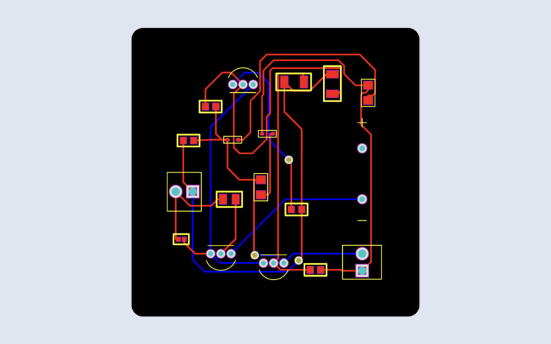
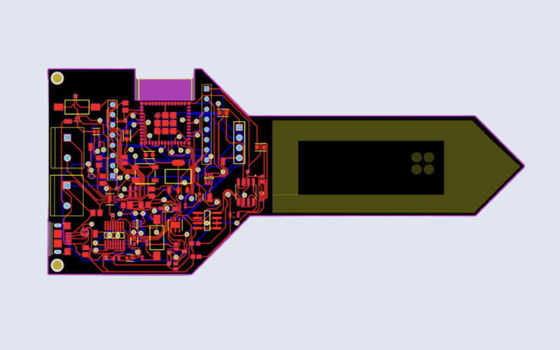
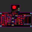
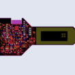
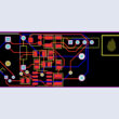
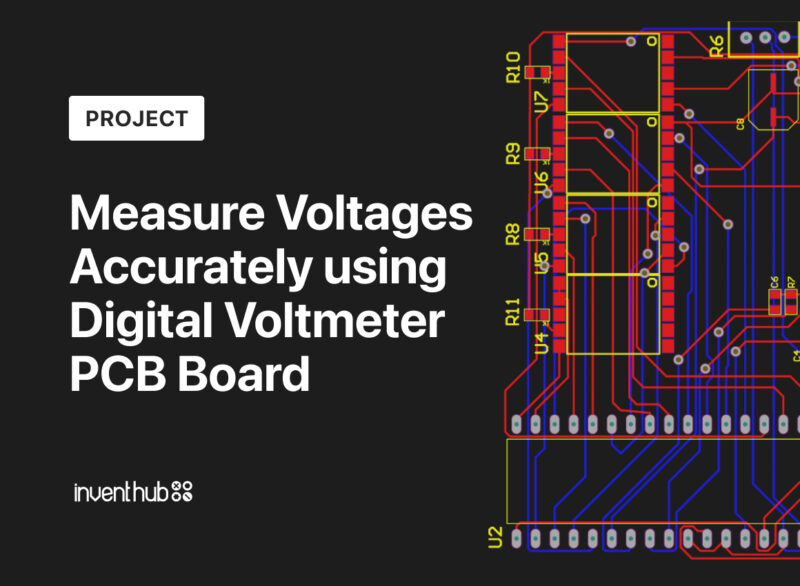
Schematic and PCB:
In Altium Designer, I have implemented the schematic diagram. I have designed the symbols and footprints in schematic and PCB libraries. After creating the schematic, I have uploaded my schematic file online on Inventhub, users can view or download the file to implement my design.
After completing my schematic, I have converted my design into a PCB file where I can design my board and can view it in 3D. I have uploaded the PCB file on Inventhub where I can explore my design in different layers that will also help me to focus on a specific layer of my board. I can view the previous changes I have made or the added or removed components in my design.
Supply Chain Management:
I have created the symbol and footprint of each component. Then I have uploaded them on Inventhub. Each component is attached to its supply chain. While designing the PCB board it is important to take care of the footprint and dimensions of each component. Footprints should be exactly the same as per component size otherwise design will not be perfect. By connecting each component to its supply chain, I can manage my components as per availability and pricing. It can help me to improve my design and reduce the cost of product.
Design for Manufacturing:
I have uploaded the release file of the design on Inventhub. This file contains all my design files in a ZIP file format. For fabrication instead of visiting the manufacturer, I will share my project files with him. The manufacturer only needs to export the file and he can fabricate the board without any error.
If I want to restore the previous version of my design and want to use it as my current design I can go to the revisions of my project where I have uploaded every edit of my design on Inventhub. I can easily go to the specific version of my design and can reuse it. The backup files of my design are available on Inventhub for the users.
Bill of Materials:
After getting the fabricated board I can embed components on it. I have created a Bill of Material on Inventhub which consists of all my component details with manufacturer and supplier details. My component provider can export the file in CSV format and can deliver my components. The total cost of the components is also being calculated automatically as per my choice of distributor and quantity. For this project, as per my BOM details the cost is $21.499 which is affordable.
To get complete how-to and detailed information on the project design and implementation visit this link: