Hardware Components:
| 1. | Infrared LED | x6 |
| 2. | RELAY DC 12V | x1 |
| 3. | CD4018 | x1 |
| 4. | NE555 | x1 |
| 5. | DC JACK | x1 |
| 6. | IRFZ44NS | x1 |
| 7. | CA3130 | x1 |
| 8. | Switch Push Button | x1 |
| 9. | Terminal Block 2 Pos | x1 |
| 10. | Resistor 47k ohm | x1 |
| 11. | Resistor 33k ohm | x1 |
| 12. | Resistor 4.7k ohm | x1 |
| 13. | Resistor 270ohm | x1 |
| 14. | Resistor 2.2k ohm | x1 |
| 15. | Resistor 27k ohm | x1 |
| 16. | Bipolar Transistor | x1 |
| 17. | Diode | x1 |
| 18. | Capacitor 10uF | x1 |
| 19. | Resistor 10k ohm | x1 |
| 20. | Resistor 100 ohm | x1 |
| 21. | Capacitor 100uF | x2 |
| 22. | Capacitor 0.1uF | x2 |
| 23. | Capacitor 0.22uF | x1 |
Software Tools:
- Inventhub
- Altium Designer
Design overview:
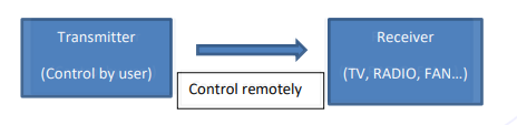
This is a simple remote controller circuit consisting of two main parts:
- Transmitter
- Receiver
These kinds of units are used to control home appliances remotely. The user can handle the transmitter side and the receiver side should connect to any type of load like TV, light, Fan, etc.
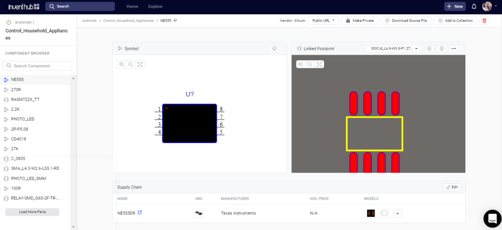
NE555 Timer IC:
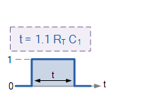
This is the one of basic timer IC in the electronic world. Its main function is to generate pulses. There are three main modes of this timer IC. They are astable, monostable, and bistable modes. We are using astable mode for our case. This mode can generate a continuous pulse (Pulse stream). Let’s discuss the difference between the operating modes of the NE555 timer.
- The astable mode works as an oscillator circuit, in which output oscillates at a particular frequency and generates pulses in a rectangular waveform

- In the monostable mode of operation, the duration of the pulse is determined by the R-C network, connected externally to the 555 timer
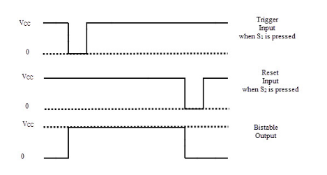
- A Bistable multivibrator is a type of circuit which has two stable states (high and low). It stays in the same state until and unless an external trigger input is applied.
I have uploaded the symbol and footprint of NE555 timer IC online on Inventhub for the users so that they can view or download it.
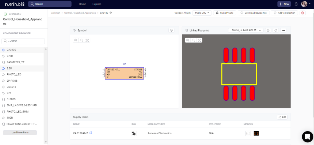
CA3130 Operational Amplifier IC:
This is a CMOS operational amplifier. Basically, it can amplify a small input signal. This IC acts as a voltage follower, peak detector, photodiode sensor amplifier, comparator, and Timer(monostable). In our case, we are using this IC for the operation of Amplification and comparator. I have uploaded the symbol and footprint of this IC online on Inventhub for the users so that they can view or download it.
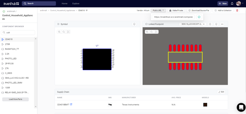
CD4018 CMOS Counter IC:
The CD4018 is a presettable Counter IC and it is used for various applications like fixed and programmable counters, programmable decade counters, frequency division, Counter control, and counter timers. I have uploaded the symbol and footprint of CD4018 CMOS IC online on Inventhub for the users so that they can view or download it.
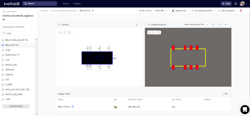
DC 12V Relay (DPDT):
This device is commonly used for switching. We are using an 8-lead relay device. It has two leads to energize the coil, two leads for common, two leads for Normally open(N/O), and two leads for Normally close(N/C). The nominal supply voltage is 12Vdc. I have uploaded the symbol and footprint of the relay online on Inventhub for the users so that they can view or download it.
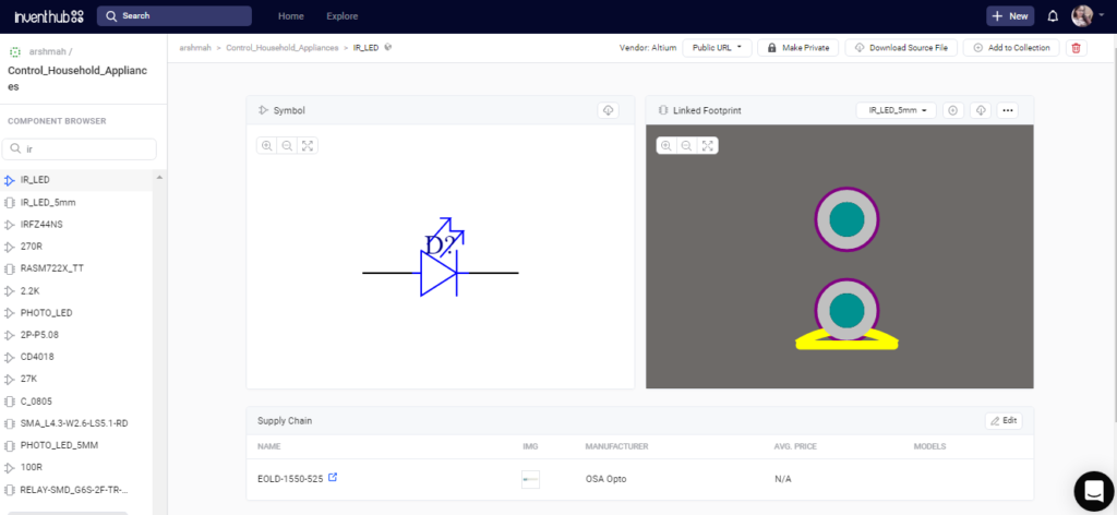
IR LEDs:
Infrared led emits infrared radiation in all directions and cannot be captured in our visible range. For the users, I have uploaded the symbol and footprint of the LEDs online on Inventhub so that they can view or download it.
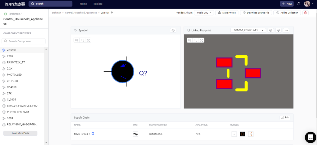
2N5401 PNP Transistor:
A PNP transistor needs a small base current and negative voltage to control a much larger emitter-collector current. This transistor can be handled a maximum 600mA collector current (Ic, 600mA). I have uploaded its symbol and footprint online on Inventhub for the users so that they can view or download it.
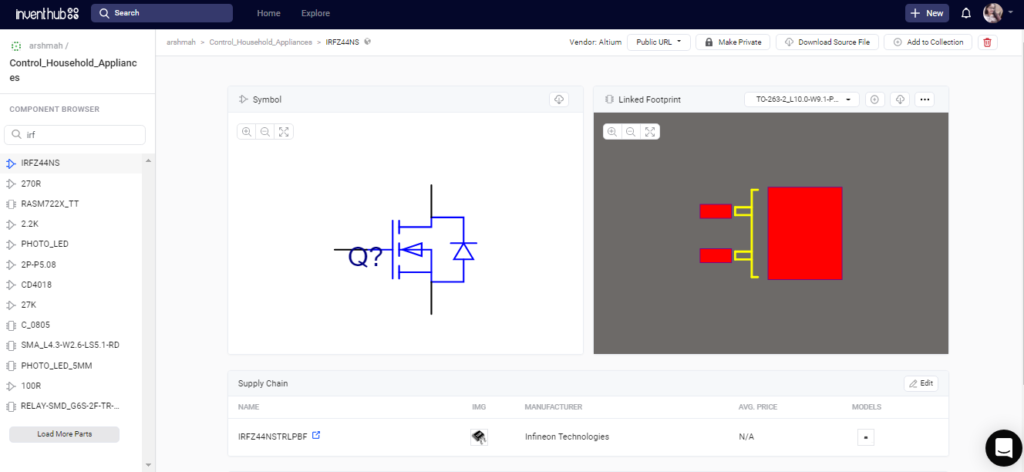
IRFZ44 MOSFET:
This is the most popular power MOSFET. It can manage fast switching. In our case, we are using this for control 12V relay. For the users, I have uploaded the symbol and footprint of this MOSFET online on Inventhub so that they can view or download it.
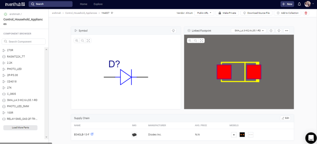
1N4007 Rectifier Diode:
This is a general-purpose silicon rectifier diode. It can handle 1A forward current. In our case, we are using this diode to protect power MOSFET from back EMF of relay. I have uploaded its symbol and footprint online on Inventhub for the users so that they can view or download it.
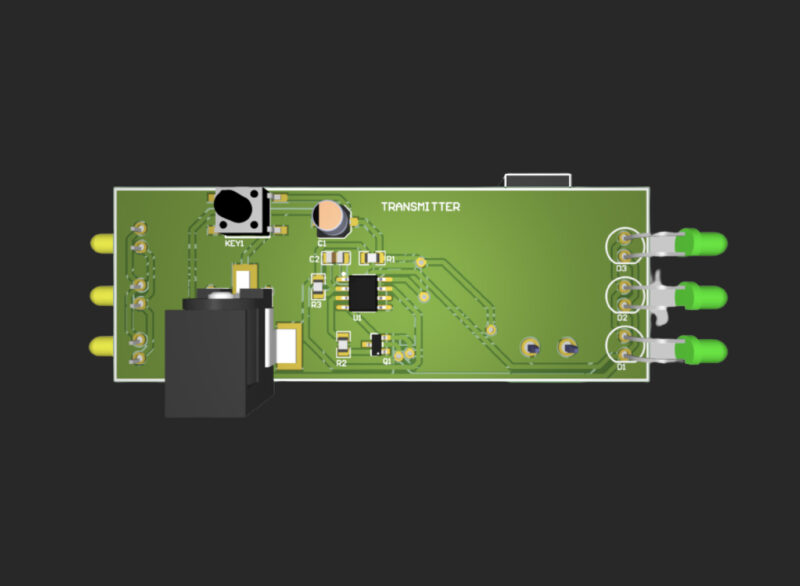
Working of Circuit:
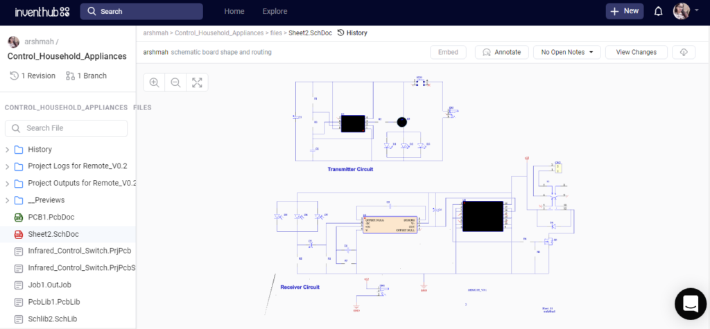
Transmitter:
When the switch is pressed, the circuit will be powered on by a 9V battery through CN1. Instantly, NE555 operates as an astable mode. It means the output gives continuous pulses (frequency 458.6 Hz).
F (Frequency) = 1.44 / (R1/2R3). C2
where R1= 27k, R3 = 2.2k, C2 = 0.1uF
Then Q1 transistor bias according to the output pulses and operate IR led with producing radiation. The resistor R2 is used to limit the current to the base of the transistor and the capacitor C1 is used to smooth the input battery power supply.
Receiver:
When gives the 12V supply through the CN2 connector, the receiver circuit is ready to detect the infrared signals from the transmitter circuit by using photodiodes. Then photodiodes biasing with support of radiation and produce leakage current. This current is supported to charge the C5 capacitor and also this current goes to the inverting input of CA3130 op-amp. The output of the op-amp directly goes to the CLK input of the CD4018. Then the output of the CD4018 counter IC will give a HIGH trigger signal to the MOSFET driver IC. Then it will act as a switch. Finally, the 12V relay will operate. R5 resistor is used to limit the current of photodiodes. C6 and R7 are used to barrier the unwanted signals to the op-amp IC. C3 capacitor is used to get high gain from IC. R4 is used to limit the current to the MOSFET IC. R8 resistor is used to discharge the internal capacitance of MOSFET IC. D4 diode is used to avoid the back EMF of the relay.
Schematic Diagram:
I have designed a schematic diagram on Altium Designer. Then I created an empty project online on Inventhub and uploaded my schematic file there. Making project online is helpful for the users who want to implement my design. They can visually view and download it from the Inventhub easily and can directly implement the design without any error. I can also add multiple files like PCB files, BOM document file, and library files by clicking the ‘Add file’ button.
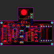
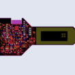
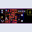
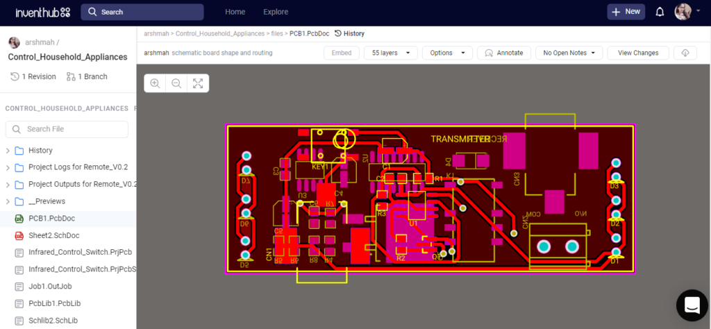
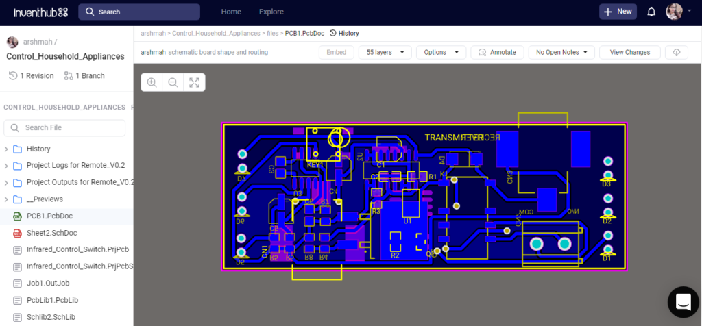
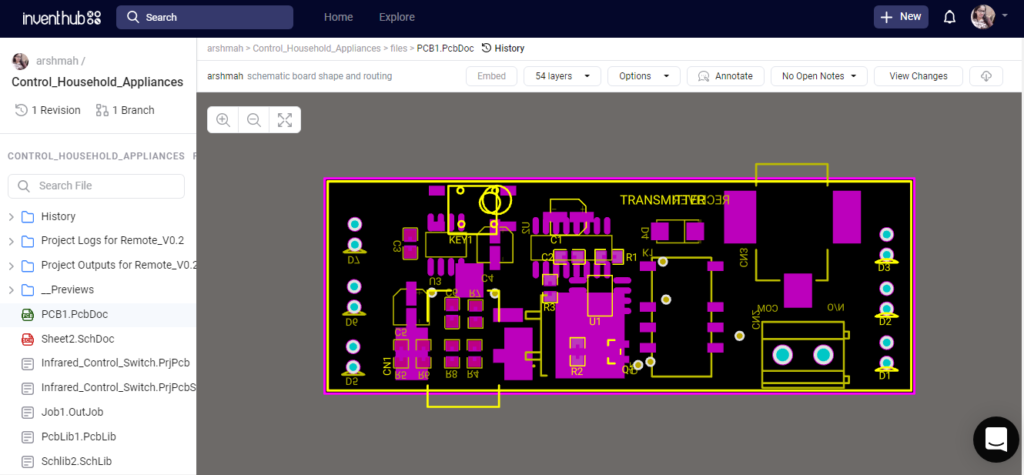
PCB file:
For the fabrication, I have converted my schematic file to the PCB file. Here I can view my board in 3D, check for the errors, and edit a shape of the board. I have uploaded my PCB file on Inventhub. Instead of visiting the manufacturer, I can send him the PCB file, he can easily download it and can fabricate my board. This is also useful for the users who want to design my board, they can view and download it from the Inventhub. I can also enable and disable the layers of the board to focus on a specific layer like the top layer, the bottom layer, and the mechanical layer.
Design for Manufacturing:
To get my whole project in one place, I have created a release file of my project after uploading all my design files on Inventhub. This file contains my schematic, PCB, library, and all history files in a ZIP file format. The manufacturer, instead of viewing and downloading each file one by one, just needs to download this release file and he can easily fabricate my PCB without making any errors.

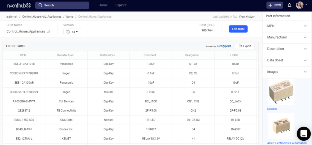
Bill of Materials:
My bill of materials contains the list of my components with all necessary details like manufacturer, supplier, part number, quantity, price, and dimensions. I have created a BOM file in Altium then I have uploaded it in CSV format on Inventhub where I can calculate the total cost of my design by selecting the ‘supply chain’ option. I can view the components and can read their datasheets also. I can select my distributor for the components depending on the price and availability of the components. Our total cost is $100. My component provider can easily download this BOM file and can deliver my components as per my design requirements.