
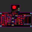
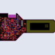
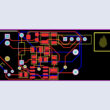
What are PCBs?
Printed circuit boards (PCBs) are a technology that generates organized connections among electronic components. Conductive pathways, or traces, made from copper sheets laminated onto a nonconducting insulating substrate are used to connect electronic components and to support the circuit board. These “printed” pathways enable the connections to be easily completed without soldering or introducing any electrical power.
Applications of PCBs
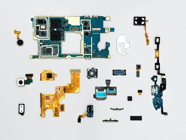
Modern technology depends on printed circuit boards or PCBs, which serve as the foundation for most electrical devices. Essentially as a foundation, PCBs can be configured in different ways to serve specific purposes and provide specific capabilities. Today, printed circuit boards are used in practically everything we come in contact with. Whether it is an appliance or a piece of landline telephone hardware, the most common component is the printed circuit board. The need for flexibility in these circuits has led to an increasing variety of applications and features available in the industry today.
Some of the applications for which you may find PCBs to be used include the following:
- Consumer Electronics, consumers depend on electronic devices for communication, safety, entertainment, and convenience in their everyday lives. Electronics are found in many consumer products ranging from mobile phones to microwave ovens to coffee makers. There are numerous applications for printed circuit boards (PCBs) in this sector. Some common use cases:
- Communications: PCBs provide the foundation for a range of devices from smartphones, to smart watches and tablets to radios.
- Computers: At the heart of every computer, navigation device, and smart phone are circuit boards. These tiny yet critical modules are essential to a large number of devices with screens.
- Entertainment Systems: TVs, stereos, DVD players, and games consoles all have something in common: they use printed circuit boards to make the magic happen.
- Home Appliances: devices like your microwave, refrigerator, alarm clock, coffee maker and other home appliances use PCBs.
- Industrial Applications, industry relies on custom printed circuit boards to help automate their businesses. From reducing human error and increasing efficiency to reducing costs, PCBs provide high-tech solutions for businesses in the industrial sector.
Here are some examples:
- Industrial Equipment: Assembly machines, presses, and ramps used in this industry are built with printed circuit boards.
- Power Equipment: From power supplies and inverters for home use to industrial applications, PCB has you covered.
- Measuring Equipment: It is a circuit board used in many different machines that is used to control the temperature, pressure and other variables that are used in the manufacturing process.
- Medical Devices, technology is changing at a fast rate and PCBs are used in almost any kind of technology. Their impact in the medical industry is astounding. They’re used as diagnostic instruments, disease treatment devices, and even monitoring devices. So as technology develops and improves more opportunities could become available.
Some of the common applications:
- Scanning Equipment: When it comes to X-Rays, CT Scans and Ultrasonic Scans, the guts of how everything works rely on a good foundation of circuit boards and copper wires.
- Monitors: The instruments that check your blood pressure and heart rate, your blood glucose meters, and other medical equipment all require circuit boards, batteries, and other electronic components.
- Medical Instruments: Medical researchers often use electronics in microscopes, control systems, compressors, and other devices that contain PCBs.
- Automotive Applications, vehicles now contain a range of advanced electronics and electrical parts that provide more functionality. In comparison, circuit boards used to feature on the older cars, only had a few electronic circuits for the essentials; similarly, circuit boards have come a long way and now we find them in many uses.
Some of the common applications include:
- Navigation: We use PCBs for many modern devices such as navigation systems. These systems contain the small printed circuit boards that the devices require to function.
- Media Devices: With their modern electronics, today’s vehicles have hands-free calling, keyless entry and more, which makes driving and using your car safer. This is all with using electronic parts.
- Control Systems: Circuit boards are powerful tools used to monitor and manage components of a vehicle. With circuit boards, advanced car control systems become easy to make and can be tailored to a specific type of vehicle.
- Proximity Monitors: Modern automobiles are fitted with sophisticated system to increase safety and overall driving enjoyment. As a result, electrical and electronic components play a crucial role in braking, acceleration, diagnostics, climate control, and many other systems.
Types of pcb board
In the modern electronic industry, printed circuit boards (PCBs) are available in a variety of shapes and sizes. These circuit boards can be large or small and can carry out various functions in products such as portable devices, communications systems and computers. Different types of printed circuit boards are categorized according to their function. There are many different types of printed circuit boards in use today and they vary in size and shape.
Single sided or Single layer PCBs:
Single sided printed circuit boards are a variant of PCBs where only one side is used for conducting circuitry. The other side allows for easy incorporation of other components. The first printed circuit board technology, single-sided boards were used beginning in the mid 1900s and consist of a substrate layer, a conductive metal layer, and a protective solder mask and silk screen.
They remain one of the most commonly used circuit boards. These boards are the simplest printed circuit board (PCB) technology available and also have low-cost production of most electronic devices.
Benefits of single sided PCBs
Single-sided circuit boards have relatively simple designs, requiring fewer resources and allowing for lower manufacturing costs. This combination allows for affordable, high-quality products to be produced quickly and in large quantities. Additionally, this enables the production of boards in large numbers with ease, whereas multi-layer boards require more time and effort to produce.
Single sided PCB applications
Circuit boards that are easy to produce and ideal for simple, low-density designs are commonly produced. They can be found in all sorts of electronic devices—often the ones you take for granted, such as radio and stereo equipment, and printers. Because of their low production costs, single sided PCBs are a choice for many. However, it is important to consider your design requirements and whether a single layer board will work for you.
Double sided or Double layer PCBs:
Popular for printed circuit boards, double sided PCBs allow for increased complexity in the design of the PCB, and thus for the products themselves. Conductive copper and components can be mounted on both sides of double sided PCBs, whereas single sided PCBs have this surface area dedicated to the board itself. These boards enable designers to route traces closer together because they can use vias to alternate between the top and the bottom layer. Drilled holes allow electronic circuits on one side of a board to be connected to the other, which can be useful.
Connection of boards:
On some circuit boards, components are connected with surface-mount technology; on others, the connections are made using through-hole technology. Double-sided PCBs share the same layers as single-sided PCBs: a substrate, copper layer, silkscreen, and solder mask. Both sides of the board are used instead of one in this case.
Benefits of double-sided PCBs:
Double sided PCBs are useful because of their high level of flexibility and ease of use. They also allow for increased circuit density since components can be placed on the second layer. Although double-sided boards are more complex, this results in smaller PCBs that are great for lighting or car dashboard integration. This saves money because smaller products can be made and sold at a reduced cost.
Multilayer PCBs:
Many printed circuit boards only have one or two conductive layers. These PCBs are designed and manufactured using either blank pads, double sided or a single-sided base material (substrate). A multi-layer PCB on the other hand, is not created based on a single layer of base material, but through at least three layers of base materials. A bunch of double-sided conductive layers exist in multilayer pcbs, separated by a corresponding number of insulating material sheets. The final PCB is bonded and laminated under high pressures and temperatures, with no air gaps that results in a sufficiently robust pcb.
Are multilayer PCBs better than double-sided?
Similar to how a car’s frame provides structure and support, multi-layer PCBs provide a solid foundation for electrical circuits. The multi-layer PCB enhances the circuit’s reliability by protecting sensitive components and ultimately creating a finished board that’s more durable and efficient with a smaller footprint. Key advantages:
- Improved durability, adding layers to a design can be a good way of building in extra protection for robust physical design.
- Overall quality, while significantly more difficult to design and assemble, the production process is thus more rigorous and attention to detail is necessary.
- High-power circuit designs, Some performance devices may require you to design your PCB with multiple layers making it better for complex designs.
- Space-saving, A circuit board’s footprint can be reduced by stacking conductive layers, allowing for larger circuits that still fit on a smaller board.
- Single connection point, there is just one input to a multilayer design instead of multiple inputs to individual pcbs.
Manufacturing and assembly of multilayer pcbs:
Multilayer PCB manufacturing is the process that is done after the single-layer PCBs are manufactured. This process involves deposition of layers of conductive paths, insulating material and other components such as resistors and capacitors etc. The process includes defining the design layout, manufacturing via a wide range of fabrication processes, assembling the components together and testing it for functionality.
The exact techniques used to produce multi-layer PCBs will depend on the shape of the finished board; in the case of a non-standard shape, the process may be more complicated to fit within the equipment and with other boards being produced. It may not be feasible to produce a bespoke shape, in which case manufacturers may have access to blank boards that they can drill into.
What are multilayer PCBs used for?
Multilayer PCBs are used in electronic devices to improve efficiency and performance. They have many advantages over single-layer PCBs and the use of these boards has increased in recent years with the increase in functionality for computers, mobile devices, medical equipment, GPS trackers, and more complex circuits.
Checkout more details on multilayer pcbs and its manufacturing process.
Rigid PCB:
A Rigid PCB is a rigid printed circuit board that allows the machine or system not to be deformed due to external mechanical force or impact. The material used in rigid circuit boards is FR-4. These boards are desired as they are extremely robust against distortion and other mechanical damage. The Rigid PCBs can easily be designed as per the requirements of the machine mechanical design and manufacturing process flow chart because of its rigidity. This makes it suitable for various industries like transportation, automotive, medical and many more.They are constructed of several layers including a substrate layer, a copper layer, a solder mask layer and a silk screen layer. These layers are joined together via adhesive and heat.
Its benefits and when to use it:
Flexible PCBs are less durable than rigid PCBs, so if you want a hardy circuit board, with more components on it, then a rigid PCB is better. They are cost effective and are able to be produced in large quantities. It also allows for increased circuit density. Rigid PCBs are popular in products where electronic components need to remain fixed and withstand high temperatures and stress.
Applications of Rigid PCBs:
They can be seen in many products today which are used across various places. GPS, Computers, non-portable apparatus like x-ray machines, heart monitors, CAT scans, MRI systems and also in the aerospace industry with control instruments and proximity sensors.
Flexible PCB:
Flexible PCB is where the substrate material is a flexible circuit board. It can be bent, folded, rolled and twisted. Typically, this type of PCB (a hybrid between rigid and flexible printed circuit boards) is used in applications or products that require flexibility.
Flexible PCB manufacturing can be performed through a variety of different processes, each with its own unique price, lead time and performance characteristics. The most established processes for flexible circuit boards are thin-film printing (flex-printing), double-sided copper clad PCB lamination, and laminate coating. But the rise of continuous roll-to-roll PCB processing methods has introduced new flexible PCB manufacturing methodologies that have proved their mettle within the Industrial IoT and wearable electronics sectors, among others.”
Benefits of flexible pcbs:
There are several benefits of using flexible PCB boards for standard electronic product assembly, including size optimization and function simplicity.The nature of flex PCBs allows them to be less space-intensive and lighter in weight than most circuit boards. Flex PCBs allow a product to be more flexible, which is useful for a variety of products. Their substrates dissipate heat and can withstand high heat. Flex PCBs with their design become compatible with various types of components that may be cost-effective and small in size. These also include connectors that can adjust to their design. The best part is they use less material and packaging which allows for cost-effective replacements.
Rigid-Flex PCBs:
A Rigid-Flex PCB can bend and flex a little. This may not sound like much, but it can have a huge impact on your products. One of the problems with making mechanical stuff using electronics is that you always seem to run into space problems. Enough room is needed for your ICs and resistors, then you need room for your connectors, fuses and wire harnesses. All this takes up a lot of space and that means less room for all the mechanical parts. Rigid-Flex PCBs are 3D boards that may be folded or twisted to accommodate the shape of a product. This can be useful in medical devices where space is at a premium.
Common types of rigid-flex pcbs:
These include:
- Flex to install, it is the most common where the board is folded only once when the product is either assembled or taken apart. Although it is sturdy and stable throughout.
- Dynamic flex, it applies to a product which requires bends when in use, resulting in highly durable and can withstand multiple flex cycles.
The process is slightly different and time consuming with more complexity but it allows for more versatility and durability of the rigid-flex pcb product.
Benefits and Applications:
Rigid-flex boards are compact, and because they are lightweight, they are used for a number of applications in:
- Aerospace
- Medical
- Consumer electronics fields.
Some of the benefits include:
- Huge amount of flexibility
- Less space because of 3D
- Shock resistance
- More reliability
- Light weight
- Less solder joints resulting in better reliability of higher connection.
- Simple PCB assembly
They are able to withstand high stress environments and are a good choice for products where resilience is needed like on connector failure.
High Frequency PCB:
High frequency electronics mean using either very high frequencies or very fast switching speeds. High frequency PCBs are PCBs designed for those applications and require special techniques to ensure the signals you are trying to send get through the PCB properly.
High Frequency PCBs and its manufacturing is related to design itself. These pcbs and their designs allow passing of signals as high as 1GHz. Special-purpose PCBs may require some laminate materials and controlled impedance with additional capabilities.
Benefits and Applications:
Their benefits include:
- They are high in density and have improved signals with a frequency of atleast 1GHz , making them ideal for high speed designs.
- Their ground plane enhances the signal’s quality and reduces EMI.
- Less circuit impedance and have shielding effect
- As the between plane and trace layer there is less distance, there is no crosstalk
- With better length and trace width of pcb design of the board, high and excessive heat is avoided at high frequencies.
High frequency PCBs find themselves in various high impactful applications like:
- Medical, such as x-ray machines, health monitors, MRI, and more.
- Industrial applications, including electric drills, solar panels, inverters.
- Communication applications, including receivers, microphones, and day to day computers and cellphones.
- Others like radars, and the aviation industry.
Checkout more details on high frequency pcb designs.
High Density Interconnect (HDI) PCB:
These types of pcbs use precision based technology when it comes to manufacturing to build as much functionality in a packed small space. Many conductive layers help in doing that, micro vias with laser drilling, with detailed lines and tolerances, and laminate materials which are advanced. HDI PCBs allow for the complexity of routing with chips that have a high number of pin count and other small components. They have smaller capture pads alongside higher connection pad densities. Manufacturing of HDI PCBs requires special equipment and is time consuming, various processes and specific equipment is needed to put together high quality boards. The lamination process is complex, because there are multi-layer boards built and constructed with high density routed layers.
Applications of HDI PCBs:
There can be a wide range of products across various industries that have the use of HDI PCBs. As they are used in advanced systems that include computers, they also have an impact on the medical side with their small size results in devices like imaging machines for small sized cameras, helping hospital staff with patient diagnosis, without having to worry about the quality of the picture.
Aluminum backed PCBs:
As one of the PCB types, it is used to support heavy electrical parts, like the transformer in power supply. The PCB of aluminum backed type has two sides: Aluminum plate and copper plate. Double-sided copper pcb boards can replace it but the price would be much higher than a single sided copper one.
These work in high power applications, the aluminum build allows for heat dissipation. Aluminum backed PCBs offer rigidness at a high level and thermal expansion at low level, thus are ideal for use cases with high mechanical tolerance. They are used for LEDs and power supplies.
Before Going into Mass Production of PCBs:
In order to ensure your design works properly, it’s a good idea to create several prototypes before mass production. By ordering a prototype PCB, you can identify problems or errors before you spend the time and money producing the board for use. As a product design project moves through the development cycle, it may require a new type of PCB prototype with unique capabilities. In fact, an early prototype can be beneficial to define precisely what is needed from each subsequent PCB iteration.
While it looks as if building a prototype adds several steps, prototyping serves important verticals in the design process. There can be several benefits like:
- Reduced Timeline
- Manufacturing Involvement
- More reliable and detailed prototype
- Allows for individual component testing
- Reduced Cost
Before mass production, prototyping with various stakeholders can drastically improve product quality. It is very important to understand new product production, testing, complex components and designing purposes. This allows for catching of design flaws, cost-saving adjustments, and flexibility in production. Breaking down the complex design process helps in better quality products. Lets have look at the steps to design a PCB:
- Create the Schematic
- Create a Blank PCB Layout
- Schematic Capture: Linking to Your PCB
- Designing Your PCB Stackup
- Defining Design Rules and DFM Requirements
- Place Components
- Insert Drill Holes
- Route Traces
- Add Labels and Identifiers
- Generate Design Files
PCB and Manufacturing:
Designers are now responsible for designing much of the PCB layout in CAD software and then sending that layout to a PCB fabrication vendor. If a designer or engineering team doesn’t have much experience with PCB design, this process can be tedious, slow, and sometimes error-ridden. Check out the basics of pcb design of a product.
Details around the circuit board:
The first step to fabricating a PCB is to create a schematic and PCB design. The design team will discuss their design with the manufacturing partner in order to decide on the exact size and shape of the board, as well as any features that need to be included. These features may include drill sizes, panelization, or other requirements. All of this information is necessary when creating a layout for your board. Some details include:
- Board layer stackup and configuration
- Controlled impedance layers
- Minimum trace width and spacing
- Via types and structures
- Copper balancing
- PCB panelization considerations
PCB Design Completeness:
Your PCB schematic is a blueprint for the PCB layout. If the design changes during the board build, there’s a high chance that your final product will have problems. Most of these problems will be related to issues with components like traces and pads around the components. To avoid costly and time-consuming problems, it is recommended that the design be completely reviewed before the start of manufacturing. Some of the things to check off in design for moving to manufacturing:
- Engineering reviews have been performed on the circuit.
- Databases that keep track of the schematic and related layout information are kept current and synchronized.
- Board components and net connections have been placed.
- Analysis of circuits, signals, and power with their integrity are performed and reported.
- The PCB design is verified with design rules and errors are corrected.
- Because the Bill of materials (BOM) is subject to change, it’s reviewed for current and available components.
- Error-free assembly rules in design for manufacturing (DFM) are reviewed.
Design data for manufacturing:
After each design has gone through rigorous in-house testing and the design team is satisfied with its performance, a full set of fabrication and assembly data files are generated and submitted to the contract manufacturer. These files will be used by your PCB company to conduct their design reviews, at which point they will send them onward to their fabricator, who will quote your final build. These data files would look like:
- Gerber files or other board image files
- Manufacturing drawings for fabrication and assembly
- Bill of materials (BOM),
- Component XY locations (pick & place)
- Test point locations
- Netlist
- Schematic
When you’re ready to get a contract manufacturer to start producing your PCB assemblies, the first step is to simply review your specifications and make sure all the materials are present. Checkout how Design for manufacturing is important.
PCB Designing Software:
PCB designing software is a tool to create, edit and manipulate PCB artwork. It is an essential part when you are in the PCB design process. There are many PCB design softwares in the market but only a few of them are popular. Among these are:
- Eagle
- Multisim
- EasyEDA
- Altium Designer
- KiCad
- CircuitMaker
- OrCad
- Allegro
- Pads
PCB Materials:
Semiconductor device manufacturing is a high-precision, high-technology process that uses many different types of materials in the fabrication equipment., it is often difficult for designers to know which materials are compatible and which are not, which will perform to expectation, and how they may affect the electrical performance, mechanical integrity and thermal durability of their designs.
Some basic components of a standard PCB:
- Prepreg
- Laminate
- Copper foil
- Soldermask
- Nomenclature
- Final finish
Laminates are laminated sheets in layers used to hold components and other materials onto a board. The material choice will affect the end product’s thermal and electrical properties. There are many types of thermal and electrical factors that can determine which laminate is best for a certain component or PCB design.
Tips on Designing PCBs:
Designing a printed circuit board requires the coordination of multiple steps, each of which is vital to create a functional, reasonably priced product. The manufacturing stage begins with the placement and routing of components on both sides of a multi-layer PCB. Some things to keep in mind:
- Don’t Rely On Your Autorouter
- Understand Your Manufacturer’s Specifications
- Figure Out Your Trace Widths
- Leave Enough Space Between Traces
- Avoid Using 90 Degree Trace Angles
- Leave Room Between Traces and Mounting Holes
- Always Create a Ground Plane
- Make Your Power and Ground Traces Wider
- Use Vias to Remove Heat
Even though designing a PCB might not seem too difficult, it’s critical to check the accuracy of your work on a prototype or “pre-production” PCB. It’s much easier to find errors when you can see the board in person instead of staring at designs on a computer screen.
PCB Design and Remote Work:
PCB design is a tricky process. It requires a creative thought process and a ton of work to bring a design from start to end. From the moment you think of your PCB idea, to having a board in your hands, you need to work at it quickly and efficiently. While there are many options for PCB design (Screen printing, etching, etc.), the world is moving at a fast pace to make PCB designs through remote collaboration. As we see from the whole process of how it involves various stakeholders and the amount of data with its iterations leads to always keeping up with several processes which make it difficult to manage. The total cost of ownership of inhouse systems is very high with big and small companies not being able to innovate quickly and spending lots on infrastructure to maintain and scale. Companies are starting to embrace cloud tooling to enable better work in the hardware electronics industry in a borderless fashion.
Inventhub connects all the electronics product design resources — people, tools, design data, component libraries, bill of materials, manufacturing — with a secure cloud based data management solution. Providing hobbyists, professionals and teams the ability to collaboratively design and deliver high quality products.
Checkout how you can modernize your electronics hardware development process.