
Hardware Components:
| 1. | Capacitor 1uF | x4 |
| 2. | Capacitor 100nF | x16 |
| 3. | Capacitor 18pF | x2 |
| 4. | LED SMD | x2 |
| 5. | Schottky Diode | x1 |
| 6. | USB C Cable connector | x1 |
| 7. | Connector header | x1 |
| 8. | Connector 10 pins JTAG | x1 |
| 9. | Inductor 22R | x1 |
| 10. | Resistor 0805 5.1kohm | x1 |
| 11. | Resistor 0805 2.2kohm | x1 |
| 12. | Resistor 0805 12kohm | x1 |
| 13. | Resistor 10kohm | x1 |
| 14. | Resistor 0805 680ohm | x1 |
| 15. | Test point | x4 |
| 16. | FPGA ICE40 | x1 |
| 17. | IC 93LC56B/P | x1 |
| 18. | Level Shifter 74AHCT541DGVR | x2 |
| 19. | IC FT232HL-REEL | x1 |
| 20. | IC Flash SPI | x1 |
| 21. | IC Linear Voltage | x2 |
| 22. | Crystal 12MHz | x1 |
Software Tools:
- Altium
- Inventhub
FPGA Chip ICE40UP5K:
FPGA stands for Field Programmable Gate Array. They are semiconductor devices that are based around a matrix of configurable logic blocks (CLBs) connected via programmable interconnects.
The ICE40 chip is an ultra-low-power FPGA and sensor manager designed for ultra-low power mobile applications, such as smartphones, tablets, and hand-held devices.

Features:
FPGA chip ICE40UP5K has the following features:
- An advanced 40nm low power process
- Embedded Memory up to 1024 kb Single Port SRAM and up to 120 kb system Embedded Block RAM which is efficient in displaying images
- It provides controls for driving the 24 mA LED Sink driver, including color controls, LED ON/OFF time, and breathing rate.
- Ultra-Small Form Factor. As small as 2.15 mm × 2.55 mm
- It also provides flexible, reliable, and secure configuration from on-chip NVCM (Non-Volatile Configuration Memory)
- It has two On-Chip Oscillators one is a low-frequency oscillator of 10 kHz and the other is a high-frequency oscillator of 48 MHz
Applications:
The benefit of using FPGAs is that they can be reprogrammed to desired application or functionality requirements even after manufacturing. That is why they are preferred to use for different applications. Their efficiency is high as compared to other devices. FPGAs are based on digital circuits consisting of thousands of gates. ICE40 is useful in different applications:
- It is used in Voice Recognition Application
- In Smartphones, Tablets, and Consumer Handheld Devices
- For Multi-Sensor Management Applications
- For USB 3.1 Type C Cable Detect / Power Delivery Application

Image processing:
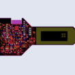
In this project, I have used an application of the FPGA that is image processing. In image processing, we use a digital computer to process the digital images like we can enhance them or view them to get some useful information. I have designed a PCB module to drive an LED display. This LED display will display the images or gifs. This display can be driven using some other microcontrollers but the reason is that they do not have onboard memory to be constantly refreshed to display an image while changing different colors. An FPGA has a feature of lots of onboard memory that helps in displaying the image without any delay.

BOM file:
For hardware components, I have created a BOM file online on Inventhub where I have mentioned each and every detail of my components like names, footprint, library, and quantity. To embed components on my PCB board I can send this file in CSV format to the component provider. He can download the file and can deliver my components as per my design requirements.

Description:
This FPGA PCB module consists of the following major components to drive an LED matrix:

- IC 93LC56B:
It is a 2Kbit low voltage EEPROM (Electrically Erasable Programmable Read-Only Memory) used for communication. It can retain the data for the long term. It consists of an ORG pin connected to the Vcc. If the Vcc is below 1.5V it will not start the operation. This IC provides protection against data if some programming accidentally happens during the normal operation. It is an 8 pins IC.

- IC 74HC5 Level Shifter:
This shift register is also used for communication. It is an 8-bit serial-in parallel-out protocol. It receives data through serial in and sends data through parallel-out configuration. If it is not used then the matrices will not work accurately. LEDs need low voltages to work like 5V so this level shifter will shift the level of voltages from high to low.

- IC FT232HL:
The FT232H is a single channel USB 2.0 Hi-Speed (480Mb/s) to UART/FIFO IC. It has the capability of being configured in a variety of industry-standard serial or parallel interfaces. UART transfer data rate up to 12Mbaud. It has a high transfer data rate necessary for better results of images or gifs. It is a compact 48-pin Lead-Free LQFP or QFN package.

- SPI Flash IC:
It is also known as flash storage. It is used to store and transmit data mostly used in portable devices. It is also popular in industrial as well as a common level like in mobile phones, laptops, tablets, and embedded devices in industries.

Schematic Design:
For the design implementation, I have decided to work on Altium which is very useful and efficient for complex designs. After creating my schematic I have uploaded my schematic file online on Inventhub for the users. Anyone who wants to implement my design can visually view or download the file from Inventhub and can implement my design.

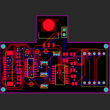
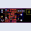
PCB:
I have implemented the PCB design of this FPGA board on Altium. It is a double layer PCB board one is the top layer and the other is the bottom layer. There is a silkscreen layer on both sides where I have written the text on my board. Autoroute in Altium allows us to route automatically but this design and its routing are quite complex so I did it carefully part by part. After completing the routing I can view the board in 2D or 3D to get an idea of how it will look after fabrication.
Once I have done designing my board I have uploaded the PCB design file online on Inventhub. The manufacturer can view or download my PCB design file to fabricate my board without any error.

FPGA Programming To Drive LED Matrix:
LED Matrix:
An LED matrix is made up of small dots to form the resolution of the display. The digital display of LED is made up of three basic colors i.e. Red, Green, and Blue named as RGB Matrix. They are also known as sub-pixels because by changing which sub-pixels are lit, and how brightly, the display can create any color.
The RGB matrix has 16 pins some of them are for RGB colors, some are for control pins (clock, latch, and blank), and the rest of them are for address pins.
RGB Matrix Driving Framework:
The framework to drive LED matrix works in three steps:

1- Firstly, fetches the data in the form of frame buffer memory which means each color has its own address and space to be fit in the frame. Split them into 64-bit row data
2- Secondly, transmit this data through the data transmitter to read it and clock it
3- Lastly, wait for the correct timing before the next row of data can be sent. This will create an RGB matrix with the display of an image of gifs with multiple colors
For the complete FPGA LED matrix driving code refer to the link below: